
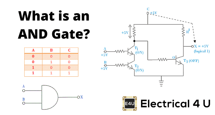
- AND Gate Definition: An AND gate is a digital logic gate that outputs high only when all its inputs are high.
- Logical Operation: This gate uses logical multiplication; the output is low if any input is low, and high only if all inputs are high.
- AND Gate Circuit Diagram: Essential for understanding how AND gates can be constructed using diodes or transistors to manipulate electrical signals.
- IC Implementation: AND gates are implemented in integrated circuits like the 7408 for TTL and 4081 for CMOS, each offering multiple gates in a single package.
- Truth Table Utilization: Truth tables are crucial for visualizing the output of AND gates based on different input combinations, aiding in circuit design and troubleshooting.
What is an AND Gate?
An AND gate is a logic gate having two or more inputs and a single output. An AND gate operates on logical multiplication rules. In this gate, if either of the inputs is low (0), then the output is also low. If all of the inputs are high (1), then the output will also be high. An AND gate can have any number of inputs, although 2 input and 3 input AND gates are the most common.
Many integrated circuits use this logic. First, let’s understand how an AND Gate’s output reacts to its inputs.
There are two binary digits – 0 and 1. We just told that an AND gate performs a binary multiplication of binary digits. In multiplying 0 with 0 we will get 0, 1 with 0 or 0 with 1 we will get 0. Only we get 1 when 1 is multiplied by 1.
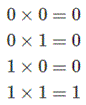
In other words, an AND gate is a digital device that produces high output only when all inputs are high and produces low output under all other inputs conditions. A high digital signal means logically 1 and a low digital signal means logically 0.
An AND gate may have any number of input probes but only one output probe.
2 Input AND Gate
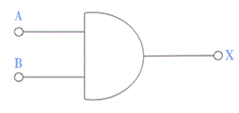
The symbol for a two-input AND gate is logically represented as:
Where A and B represent the input of the gate and X represents the output. A, B, and X can either be 0 (low) or 1 (high) logically.

The logical operation of AND gate hence can be represented as:
All multiplication combinations of A and B can be represented in tabular form in a truth table. Truth tables list the output of a particular digital logic circuit for all the possible combinations of its inputs. The truth table of a 2 input AND gate can be represented as:
3 Input AND Gate
If instead of two inputs there are three inputs, this changes the logical symbol and truth table of the AND gate.

The logical symbol of a 3-input AND gate is represented as:
The truth table of a 3 input AND gate is:

In digital electronics, other logic gates include NOT gates, OR gates, NAND gates, NOR gates, XOR gates, XNOR gates.
AND Gate Circuit Diagram
AND Gate Diode Circuit Diagram
Normally an AND gate is designed by either diodes or transistors.
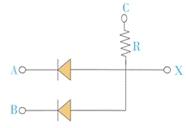
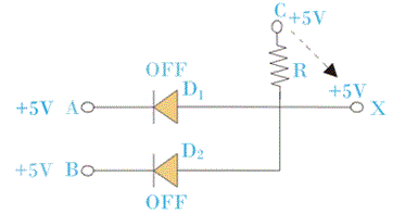
When diodes are used to design AND gate, it is called a diode AND gate. The basic circuit of a diode AND gate is shown below
In the diode circuit, we apply +5V at point C. If +5V is also applied to A and B, both diodes become reverse biased, acting as if they are OFF or an open circuit.
In this situation as both diodes are OFF, no current will flow through resistor R and voltage of C (+5V) will also appear at X. As the supply voltage +5V appears at X, the output of the circuit is considered as high or logical 1.
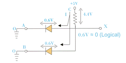
Now, if either point A or B or both are applied with 0 Volt or they are grounded, the respective diode will become forward biased and hence behaves as ‘ON’ or short-circuited. In this condition, supply voltage +5V at point C will get a path through either of diodes or both to the ground potential.
As the current flowing from C to the ground through resistor R, the entire 5V will be dropped across the resistor and hence the voltage at X will become low or logically zero.
The diodes in the forwarding biased condition do not behave as an ideal short circuit; some voltage drop will be there across the forward biased diodes which are equal to forward bias voltage.
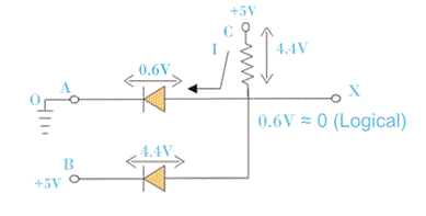
This voltage drop will appear at X during low output condition, so the practically low output will not be 0V it is rather 0.6 to 0.7V which is ideally considered as zero.
AND Gate Transistor Circuit Diagram
An AND logic gate can also be realized from the transistor AND gate. The transistor circuit diagram for an AND gate is shown below:
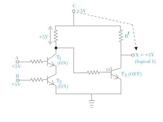
In this circuit, if A, B, or both are grounded or at 0V, transistors T1 and T2 or both will be in the OFF state.
This is because terminal A and B are base terminal of transistor T1 and T2 respectively. Zero base voltage makes a transistor OFF. As the path through T1and T2 is an open-circuited base of transistor T3 enough potential to makes T3 ON.
The current then starts flowing the supply to the ground through T3. As a result, the entire supply voltage will drop across R1, and the potential of terminal X will become low or logical zero.
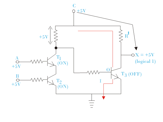
If any of the transistors T1 and T2 are in OFF condition, the same result will come at output X as both the transistors are in series.
Now we will check what will be the logical value of X if both A and B are at high logical value. If we apply +5V at both A and B i.e. at the base of transistor T1 and T2 respectively.
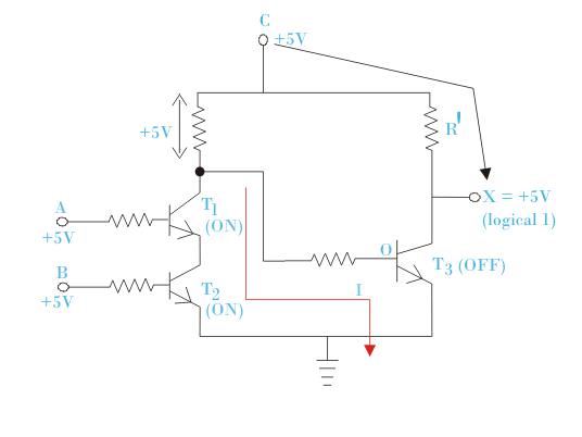
This scenario turns transistors T1 and T2 ON. The supply voltage drops across R, making the base potential of transistor T3 zero, thus turning T3 OFF. Consequently, the +5V supply appears at X, making X logically high.
AND Gate IC 7408
For AND Gate IC number in TTL is 7408. 7408 is Quad 2- input IC where four gates are present together. Let us have a look at the internal diagram of 7408.
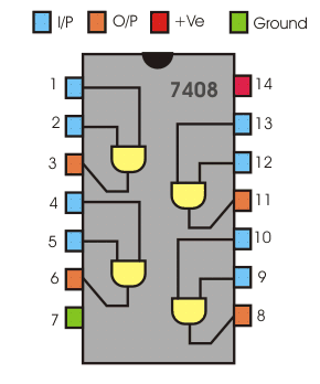
Here pins 1, 2 are the inputs of the first gate whose respective output is 3. Again 4 and 5 are the inputs of the second gate whose output is at pin 6. The inputs of the fourth are pin 12 and 13 and pin 11 is its output.
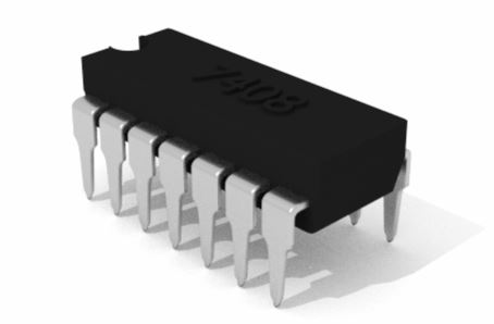
Pin 14 is the supply input which can be a maximum of 5.2 volt D.C. if input voltage be more than this it may cause damage to the IC.
AND Gate IC 4081

In CMOS logic i.e complimentary MOSFET logic I.C number of AND Gate is 4081. This IC also has two inputs and one respective output. In this IC there are also 4 gates together. Now see the below internal diagram of this circuit to make it more clear.
Pin 1 and 2 are the inputs of the first gate whose output is in number 3. Again Pin 5 and 6 are the inputs of the second gate whose output is at Pin 4. pi number 7 is grounded. Pin 8 and 9 are the inputs of the third gate whose output is at pin 10.
Again pin 13 and 12 are the inputs of the fourth AND gate whose output is at pin number 11. Pin 13 and 12 are the inputs of fourth AND Gate whose output is at pin number 11. Pin number 14 is a power supply where a maximum 5.2-volt direct current supply can be given to activate the IC.
Applying too much voltage can damage the IC. It’s important to note that the internal circuitry of CMOS and TTL technologies differs significantly.


