- BJT Definition: A Bipolar Junction Transistor (BJT) is defined as a three-terminal semiconductor device that amplifies or switches electrical signals.
- Types of BJTs: There are two types of BJTs—NPN and PNP—each with different arrangements of n-type and p-type materials.
- How BJT Works: A BJT works by using a small input current at the base to control a larger current between the collector and emitter
- Modes of Operation: BJTs can operate in three modes—Common Base (CB), Common Emitter (CE), and Common Collector (CC)—each affecting the voltage and current characteristics.
- Applications of BJTs: BJTs are used in high-frequency applications, amplifiers, and switches due to their superior transconductance and output resistance.
What is a BJT?
A Bipolar Junction Transistor (BJT) is a three-terminal semiconductor device whose two closely coupled p-n junctions can amplify or switch an electrical signal. The three terminals are the emitter, base and collector. Engineers often describe a BJT as a current-controlled device because a small base current is associated with a much larger collector current in the forward-active region. At the device-physics level, however, collector current depends strongly on the base-emitter voltage. A BJT is a type of transistor in which both electrons and holes take part in operation.
In a correctly biased amplifier circuit, a small change at the base controls a larger change in collector current. A load then converts that current change into an output voltage. The extra signal power comes from an external DC supply, not from the input signal itself.
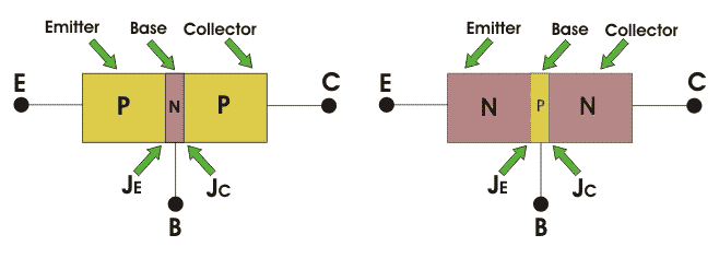
There are two polarities of bipolar junction transistor: NPN transistors and PNP transistors. Each has an emitter, base and collector.
JE identifies the emitter-base junction, while JC identifies the collector-base junction. In forward-active operation, the emitter-base junction is forward biased and the collector-base junction is reverse biased. Other bias combinations place the transistor in cutoff, saturation or reverse-active operation.
NPN Bipolar Junction Transistor
In an n-p-n bipolar transistor (or npn transistor), a thin p-type base lies between an n-type emitter and an n-type collector. The diagram below shows this structure.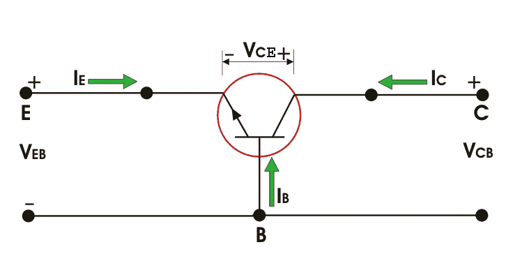
IE, IB and IC denote the emitter, base and collector currents. VEB, VCB and VCE denote terminal voltages. In the table, IE is negative for forward-active NPN operation under the stated sign convention. The listed voltages and currents are positive when directed into the device and negative when directed out.
| Transistor type | IE | IB | IC | VEB | VCB | VCE |
| n-p-n | – | + | + | – | + | + |
PNP Bipolar Junction Transistor
In a p-n-p bipolar junction transistor (or pnp transistor), a thin n-type base lies between a p-type emitter and a p-type collector. The diagram below shows this structure.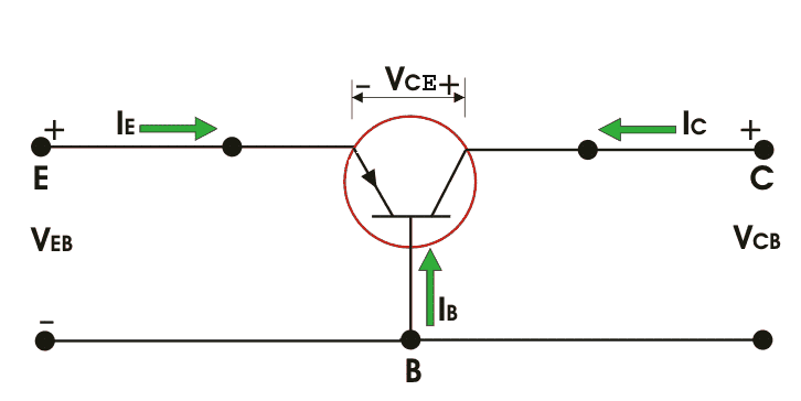
With the sign convention used here, conventional current enters the PNP transistor through the emitter and leaves through the base and collector. In forward-active operation, its emitter-base junction is forward biased and its collector-base junction is reverse biased. The table records the resulting current and voltage signs.
| Transistor type | IE | IB | IC | VEB | VCB | VCE |
| p – n – p | + | – | – | + | – | – |
Working Principle of BJT
The figure shows an NPN transistor in the forward-active region. In this condition, the base-emitter (BE) junction is forward biased and the collector-base (CB) junction is reverse biased. See transistor biasing for the circuits that establish these voltages. The forward-biased BE junction has a narrower depletion region than the reverse-biased CB junction.
Forward bias lowers the BE junction barrier and injects electrons from the heavily doped emitter into the base. The base is thin and lightly doped, so only a small, device-dependent fraction of these electrons recombines with holes there. This recombination contributes to the base current.
Most injected electrons diffuse across the base and are swept into the collector by the reverse-biased CB junction, forming collector current. Conventional current points opposite to electron flow. Applying KCL gives the terminal-current relationship shown below.
The base current is normally much smaller than the emitter and collector currents in forward-active operation.
Electrons are the principal injected charge carriers in an NPN transistor, while holes are the principal injected carriers in a PNP transistor. The name bipolar refers to the participation of both carrier types. A PNP device follows the same transport principle with voltage polarities and conventional-current directions reversed.
Equivalent Circuit of BJT
Two back-to-back diode symbols can show the polarity of a BJT’s two p-n junctions, but they are not an electrical equivalent of a transistor. Two separate diodes do not reproduce transistor action because their junctions are not coupled through a thin shared base. Useful BJT models therefore include a controlled current source or the coupled-junction behaviour represented by the Ebers-Moll model.
Bipolar Junction Transistors Characteristics
The three terminals of a BJT are collector, emitter and base. Its measured bipolar junction transistor characteristics depend on which terminal is shared by the input and output circuits. The three standard circuit configurations for this type of transistors are
- Common Base (CB) mode
- Common Emitter (CE) mode
- Common Collector (CC) mode
All three configurations are shown below.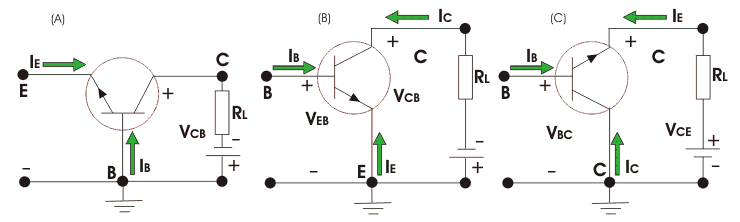
These configurations are not the transistor’s operating regions. Cutoff, forward active, saturation and reverse active are operating regions set by the two junction biases. Characteristic curves plot the relationships between terminal currents and voltages for a chosen circuit configuration. The following PNP curves use the sign convention stated above.
Common Base Characteristics
Input Characteristics
For a PNP transistor in the common-base configuration, the input current is emitter current (IE) and the input voltage is emitter-base voltage (VEB).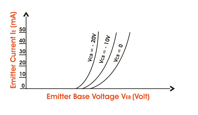
Because the emitter-base junction is forward biased, the IE-VEB curve resembles the forward characteristic of a p-n diode. At fixed VEB, IE can shift slightly when VCB changes because collector voltage affects the effective base width.
Output Characteristics
The common-base output characteristics plot collector current IC against collector-base voltage VCB, with emitter current held at several fixed values. The figure below shows these curves for a PNP transistor.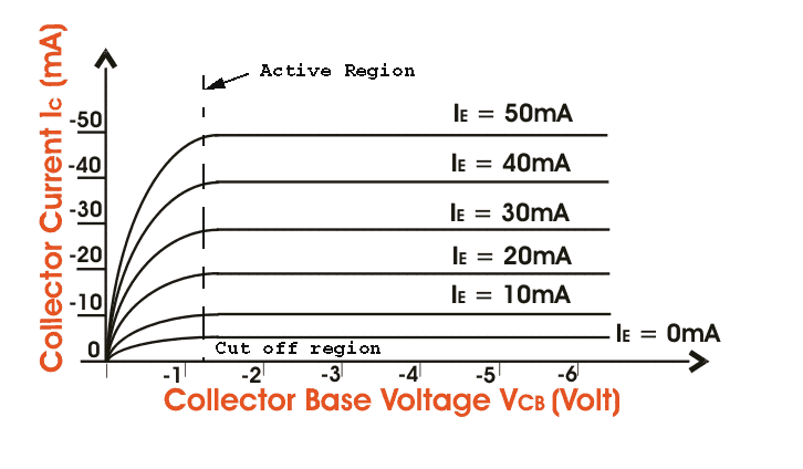
Under the table’s sign convention, IE and VEB are positive, while IC, IB and VCB are negative. The plotted regions include forward active, saturation and cutoff.
In the forward-active region, the emitter-base junction is forward biased and the collector-base junction is reverse biased. In saturation, both junctions are forward biased and the simple current-gain relationship no longer applies. In cutoff, emitter injection is near zero, although a real device still has small leakage currents.
Common Emitter Characteristics
Input characteristics
In the common-emitter (CE) configuration, base current IB is the input current and base-emitter voltage VBE is the input voltage. The input characteristics therefore plot IB against VBE, with VCE as a parameter.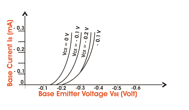
The curve resembles a forward-biased p-n junction. Changing VCB also shifts it slightly by changing the effective base width, an effect associated with the Early effect.
Output Characteristics
The CE output characteristics plot collector current IC against collector-emitter voltage VCE for several fixed values of base current IB. The figure below shows this family of curves.
The main CE output regions are forward active, cutoff and saturation. In the forward-active region, the collector-base junction is reverse biased and the emitter-base junction is forward biased. This region is used for linear amplification when the surrounding circuit establishes a suitable bias point.
In cutoff, base-emitter drive is too low to produce more than leakage current. In saturation, both junctions are forward biased, collector-emitter voltage is low and collector current is set mainly by the external circuit rather than by the forward-active current-gain relation.
History of BJTs
In 1947, John Bardeen and Walter Brattain demonstrated the first successful point-contact transistor at Bell Laboratories under a research group led by William Shockley. Shockley later developed the junction-transistor concept. Bell Labs engineer John R. Pierce proposed the name transistor before the device was publicly announced in 1948. This article focuses on the Bipolar Junction Transistor (BJT).
The name was associated with the term transresistance and chosen to fit established component names such as thermistor and varistor. It should not be read as a complete description of how every transistor transfers a signal between a Resistor and a high-resistance circuit. BJTs are made from semiconductors.
Transistors are fundamental elements of Integrated Circuits (ICs). Moores Law describes a historical industry trend in which transistor counts on leading integrated circuits grew exponentially. It is an observation about technological progress, not a physical law or a guarantee that every chip doubles its transistor count on an exact two-year schedule.
Now, why this is called junction transistor? The answer lies behind the construction. We already know what is p-type and n-type semiconductors.
Now, in this type of transistor, any one type of semiconductors is sandwiched between the other type of semiconductor. For example, an n-type can be sandwiched between two p-type semiconductors or similarly one p-type can be sandwiched between two n-type semiconductors.
These structures are called pnp transistors and npn transistors respectively, as discussed above. The term junction identifies the two p-n junctions in the device. The term bipolar indicates that both electrons and holes take part in its operation.
Applications of BJT
BJTs remain useful in discrete and integrated circuits because they can provide high transconductance for a given bias current. They are available across a broad range of voltage, current, power, noise and frequency ratings. Their output resistance is not universally better than that of a MOSFET; device choice depends on the circuit, operating point, drive power, switching loss, noise and thermal limits.
Applications include radio-frequency stages, small-signal and power amplifiers, current mirrors, oscillators, sensor interfaces and electronic switches. A BJT can also form an input or output stage within an amplifier. The correct device and bias circuit must keep its voltage, current, power and temperature within rated limits.
Bipolar Junction Transistor Amplifier
The following Bipolar Junction Transistor Amplifier example uses a PNP transistor. The DC sources establish a forward-active bias point, while small changes around that point produce the amplified signal.
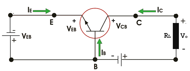
A small input change ΔVi changes the emitter-base voltage, junction barrier and emitter current by ΔIE. The corresponding collector-current change develops an output-voltage change ΔVO across load resistance RL, as represented below.
Here ΔVO is measured across RL. The negative sign follows from the voltage and current reference polarities selected in the diagram. Voltage gain AV is the ratio of ΔVO to ΔVi.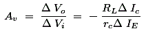

The second relation includes the transistor’s common-base current gain. For this PNP circuit, raising the emitter voltage relative to a fixed base reduces the magnitude of forward bias and therefore reduces collector current.
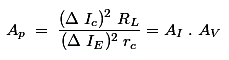
The phase relation between input and output depends on the circuit configuration and the chosen voltage reference polarities, so it should be read directly from the complete circuit rather than assumed for every BJT amplifier. Finally, power gain Ap is the ratio of output signal power to input signal power.