

- Doping Definition: Doping is the process of adding impurities to a semiconductor to change its conductive properties.
- Donor Impurities: Donor impurities are pentavalent atoms added to semiconductors, contributing extra free electrons, creating n-type semiconductors.
- N-Type Semiconductor: An n-type semiconductor has excess free electrons as majority charge carriers, introduced by donor impurities.
- Acceptor Impurities: Acceptor impurities are trivalent atoms added to semiconductors, creating excess holes, forming p-type semiconductors.
- P-Type Semiconductor: A p-type semiconductor has excess holes as majority charge carriers, introduced by acceptor impurities.
When we add a small amount of impurity to a semiconductor, it contributes either free electrons or holes. This changes the semiconductor conductivity. This process is called doping. For example, if we add pentavalent impurities (atoms with five valence electrons) to an intrinsic semiconductor, the impurity atoms replace some of the semiconductor atoms in the crystal structure. Four of the five valence electrons bond with neighboring atoms, but the fifth electron remains free.
This fifth electron of the impurity atom can be available as free electron or negative charge carrier even if a minimal amount of energy is applied. The energy required to detach the this fifth electron from its parent atom is in the range of 0.01 eV (electron volt) to 0.05 eV (electron volt). Antimony, Phosphorus, and Arsenic are usually and commercially used pentavalent impurities for a semiconductor. As pentavalent impurities contribute or donate electrons to the semiconductor, these are called donor impurities and similarly as these impurities contribute negative charge carriers in the semiconductor this we refer as n-type impurities. The semiconductor doped with n-type impurities is called n-type semiconductor.
N Type Semiconductor
When n-type or donor impurities are added to a semiconductor, the forbidden energy gap in the lattice structure narrows. Donor atoms introduce new energy levels just below the conduction band. These levels are discrete because the impurity atoms are far apart and interact minimally. In germanium, the energy gap is 0.01 eV, and in silicon, it’s 0.05 eV at room temperature. Thus, at room temperature, the fifth electron from donor atoms enters the conduction band. The increased number of electrons leads to fewer holes.
The number of holes per unit volume in an n-type semiconductor is even lower than that in the same unit volume of intrinsic semiconductor at the same temperature. This is because of excess electrons, and there will be the higher rate of recombination of electron-hole pairs than that in a pure or intrinsic semiconductor.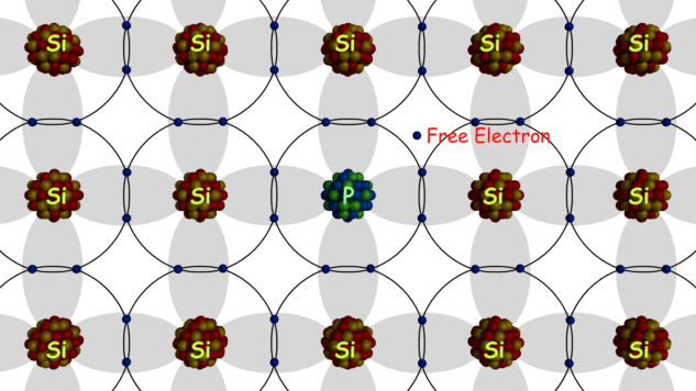
P Type Semiconductor
If instead of pentavalent impurity, a trivalent impurity is added to the intrinsic semiconductor, then instead of excess electrons there will be excess holes created in the crystal. Because when a trivalent impurity is added to the semiconductor crystal, the trivalent atoms will replace some of the tetravalent semiconductor atoms. The three (3) valance electrons of trivalent impurity atom will make the bond with three neighborhood semiconductor atoms. Hence, there will be the lack of an electron in one bond of the fourth neighboring semiconductor atom which contributes a whole to the crystal. Since trivalent impurities contribute excess holes to semiconductor crystal, and these holes can accept electrons, these impurities are referred as acceptor impurities. As the holes virtually carry positive charge, the said impurities are referred as positive – type or p type impurities and the semiconductor with p type impurities is called p-type semiconductor.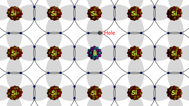
Adding trivalent impurities to a semiconductor creates a discrete energy level just above the valence band. The small gap between the valence band and this new energy level allows electrons to easily move to the higher level with a small amount of external energy. When an electron moves to this new level, it leaves a vacancy, or hole, in the valence band.
When we add an n-type impurity to the semiconductor, there will be excess electron is a crystal but it does not mean that there would not be any hole. Due to intrinsic nature of semiconductor at room temperature, there are always be some electron-holes pairs in the semiconductor. Due to an addition of n-type impurities, the electrons will be added to that electron-hole pairs and also the number of holes reduced excess recombination for excess electrons. Hence, the total number of negative charge carriers or free electrons will be more than that of holes in the n-type semiconductor. That is why in n-type semiconductor, the electrons are called majority charge carriers whereas poles are called minority charge carriers. Similarly in p-type semiconductor, holes are called the majority charge carriers and electrons are called minority charge carriers.


