

- Intrinsic Silicon Definition: Intrinsic silicon is defined as chemically pure silicon whose electrical conductivity depends on thermally generated carriers.
- Extrinsic Silicon Definition: Extrinsic silicon is defined as silicon doped with trivalent or pentavalent impurities to enhance conductivity.
- Energy Bands in Intrinsic and Extrinsic Silicon: Intrinsic silicon has equal numbers of electrons and holes, while extrinsic silicon has either more electrons (n-type) or more holes (p-type) due to doping.
- N-type Silicon: N-type silicon, created by doping with group V elements, has more free electrons as majority carriers.
- P-type Silicon: P-type silicon, created by doping with group III elements, has more holes as majority carriers.
Intrinsic Silicon
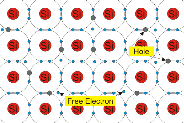
Silicon is a group 14 semiconductor with four valence electrons per atom. In a perfect crystal, each atom shares covalent bonds with four neighbours. At 0 K, ideal intrinsic silicon has a full valence band and empty conduction band, so it behaves as an insulator. At temperatures above 0 K, thermal excitation creates some electron-hole pairs. An electron promoted to the conduction band leaves a mobile hole in the valence band. Silicon’s indirect band gap is about 1.12 eV at 300 K, rather than 1.2 eV.
In equilibrium intrinsic silicon, each generated conduction electron is paired with a valence-band hole. Generation and recombination continue, but their average rates are equal at a fixed temperature. Electron concentration n and hole concentration p therefore both equal the intrinsic carrier concentration ni: n = p = ni. This equality describes an undoped equilibrium crystal; illumination, injection or non-equilibrium bias can change the carrier populations. The atomic structure is shown below.

Intrinsic Silicon at 0 K
Intrinsic Silicon at Room Temperature
Extrinsic Silicon
Controlled donor doping produces an n-type semiconductor, while acceptor doping produces a p-type semiconductor.
Common group 15 donors in silicon include phosphorus, arsenic, antimony and bismuth. Four valence electrons form bonds with neighbouring silicon atoms, while the fifth occupies a shallow donor state. Thermal energy can ionise the donor and release that electron to the conduction band. The ionisation energy is dopant-specific and is often of the order of 0.05 eV for common shallow donors. N-type silicon remains electrically neutral because mobile electrons balance positively ionised donor atoms; the word n-type identifies the majority carrier, not a net negative charge.
Donor doping shifts the equilibrium Fermi level toward the conduction band. Electron concentration rises above the intrinsic value and hole concentration falls according to charge neutrality and the equilibrium mass-action relation. Electrons are the majority charge carriers, while holes are minority carriers.
Extrinsic Silicon with Pentavalent Impurity
Group 13 acceptors such as boron, aluminium and indium have three valence electrons when substituted into the silicon semiconductor lattice. An acceptor can capture an electron from a neighbouring bond, leaving a mobile hole in the valence band. P-type silicon remains electrically neutral because mobile holes balance negatively ionised acceptor atoms; p-type identifies the majority carrier rather than a net positive charge.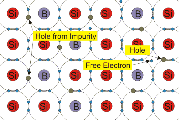
Extrinsic Silicon with Trivalent Impurity
Acceptor doping shifts the equilibrium Fermi level toward the valence band. Hole concentration rises above the intrinsic value and electron concentration falls. Holes are the majority charge carriers, while electrons are minority carriers.
Intrinsic Carrier Concentration of Silicon
Thermal excitation across the band gap creates one conduction electron and one valence-band hole. Their equilibrium concentration in undoped silicon is the intrinsic carrier concentration ni. Thus n = p = ni.
Intrinsic carrier concentration depends strongly on temperature through the band gap and the effective densities of states. Silicon’s gap is about 1.12 eV at 298 K. A common non-degenerate approximation is shown below.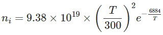
Here, T is absolute temperature in kelvin.
At 300 K, ni is about 1.0 × 1010 cm-3 for commonly used material parameters. Older references often quote 1.5 × 1010 cm-3; the exact calculated value depends on the selected band-gap and effective-density models.


