

- Zener Diode Definition: A Zener diode is a special type of diode that allows current to flow in reverse when a set voltage, called Zener voltage, is exceeded.
- Working Principle: The zener diode working principle involves a voltage-triggered breakdown that allows it to conduct electricity in reverse, providing a stable voltage regardless of input changes.
- Voltage Regulation: Zener diodes are essential for maintaining consistent voltage in electronic circuits, ensuring devices operate under stable conditions.
- Zener Breakdown vs. Avalanche Breakdown: Zener breakdown is a controlled, sharp breakdown at a lower voltage compared to the more gradual avalanche breakdown.
- V-I Characteristics: The Voltage-Current (V-I) characteristics for a Zener diode graphically show the sharp increase in current at the Zener voltage, defining its function in circuits.
Working Principle of Zener Diode
When a PN junction diode is reverse biased, the depletion layer widens. Continuously increasing the reverse bias voltage across the diode makes this layer even wider. Simultaneously, a constant reverse saturation current flows due to minority carriers.
At a specific reverse voltage, minority carriers gain enough kinetic energy from the strong electric field. These energetic electrons collide with stationary ions in the depletion layer, releasing more electrons. The process continues, generating additional free electrons through cumulative collisions. Due to this commutative phenomenon, very soon, huge free electrons get created in the depletion layer, and the entire diode will become conductive. This type of breakdown of the depletion layer is known as avalanche breakdown, but this breakdown is not quite sharp.
This cumulative effect quickly generates numerous free electrons in the depletion layer, making the diode conductive. This process, known as avalanche breakdown, does not have a sharp onset. There is another type of breakdown in depletion layer which is sharper compared to avalanche breakdown, and this is called Zener breakdown. When a PN junction is diode is highly doped, the concentration of impurity atoms will be high in the crystal. This higher concentration of impurity atoms causes the higher concentration of ions in the depletion layer hence for same applied reverse biased voltage, the width of the depletion layer becomes thinner than that in a normally doped diode.
The thinner depletion layer causes a high voltage gradient or electric field strength. Increasing the reverse voltage further leads to a point where electrons break free from covalent bonds, making the region conductive. This is the Zener breakdown. The voltage at which this breakdown occurs is called Zener voltage. If the applied reverse voltage across the diode is more than Zener voltage, the diode provides a conductive path to the current through it hence, there is no chance of further avalanche breakdown in it. Theoretically, Zener breakdown occurs at a lower voltage level then avalanche breakdown in a diode, especially doped for Zener breakdown. The Zener breakdown is much sharper than avalanche breakdown. The Zener voltage of the diode gets adjusted during manufacturing with the help of required and proper doping. When a zener diode is connected across a voltage source, and the source voltage is more than Zener voltage, the voltage across a Zener diode remain fixed irrespective of the source voltage. Although at that condition current through the diode can be of any value depending on the load connected with the diode. That is why we use a Zener diode mainly for controlling voltage in different circuits.
Zener Diode Circuit
Zener Diode is nothing but a single diode connected in a reverse bias, we have already stated that. A diode connected in reverse bias position in a circuit is shown below,
The circuit symbol of a Zener diode is also shown below.
Characteristics of a Zener Diode
Now, discussing about the diode circuits we should look through the graphical representation of the operation of the zener diode. Normally, it is called the V-I characteristics of a Zener diode.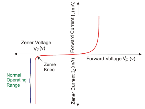
The above diagram shows the V-I characteristics of a zener diode. When the diode is connected in forward bias, this diode acts as a normal diode but when the reverse bias voltage is greater than zener voltage, a sharp breakdown takes place. In the V-I characteristics above Vz is the zener voltage. It is also the knee voltage because at this point the current increases very rapidly.
")


