

- PN Junction Diode Definition: A PN junction diode is defined as a two-terminal electronic component with one side doped with P-type impurities and the other with N-type impurities.
- Step Graded Junction: In a step graded junction, the concentration of dopants is uniform up to the junction on both sides.
- Depletion Region: The depletion region forms at the junction where free electrons and holes recombine, creating an area with no free charge carriers.
- Forward Bias: Applying a forward bias decreases the depletion region’s width, allowing current to flow.
- Reverse Bias: Applying a reverse bias increases the depletion region’s width, blocking current flow until breakdown voltage is reached.
A PN junction diode is a two-terminal semiconductor device formed around adjoining p-type and n-type regions. In this type of diode, acceptor doping makes one side p-type and donor doping makes the other n-type. The spatial dopant profile near the junction may be abrupt, often called step graded, while other junctions change gradually.
An ideal step junction has uniform doping on each side and an abrupt change at the metallurgical junction. A linearly graded model makes net dopant concentration change approximately linearly with position. At thermal equilibrium with no external voltage, majority carriers initially diffuse down their concentration gradients. Recombination and the exposed ionised dopants create an electric field whose drift current balances diffusion current.
Ionised acceptors on the p side are fixed negative charges, while ionised donors on the n side are fixed positive charges. The resulting space-charge field opposes majority-carrier diffusion. The depletion region contains far fewer mobile carriers than the quasi-neutral material outside it, although “depleted” does not mean that every mobile carrier is absent.
Forward bias makes the p side of the p-n junction diode positive relative to the n side. Connecting the positive terminal of a battery this way lowers the junction barrier, narrows the depletion region and injects minority carriers into the quasi-neutral regions. Reverse bias raises the barrier and widens the depletion region. A small reverse leakage current still flows before breakdown, so reverse bias does not block all charge.
P-N Junction Diode Characteristics
Consider an abrupt junction with donor concentration ND and acceptor concentration NA. A simple depletion model assumes fully ionised dopants, low injection and majority-carrier concentrations close to ND and NA in the quasi-neutral regions. Minority carriers, compensation, incomplete ionisation and defects require a fuller model. 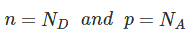
Initial carrier diffusion exposes fixed dopant ions near the junction. Their space charge produces the electric field and built-in potential. The region in which mobile carrier concentrations are much smaller than the dopant charge is the depletion region. At equilibrium, diffusion and drift occur in opposite directions with zero net terminal current. The built-in potential is also called the diffusion voltage and, under the stated assumptions, is represented below.  Applied forward voltage lowers the barrier and narrows the depletion region; reverse voltage raises the barrier and widens it. The region normally remains finite under forward bias. Its electrostatic potential and field follow Poisson Equation, whose depletion-approximation solution gives a width that depends on doping, permittivity, built-in potential and applied bias.
  Here ε is semiconductor permittivity and V is the applied junction voltage under the equation’s sign convention. Forward current comes mainly from minority-carrier injection, diffusion and recombination in the quasi-neutral regions. Silicon is an indirect-band-gap material, so recombination usually transfers energy to the lattice rather than emitting one photon per carrier pair. Under low-level injection and other ideal assumptions, the diode current is
  Here V is junction voltage, I is current, Is is reverse saturation current, e denotes elementary charge, k is Boltzmann’s constant and T is absolute temperature. Real-diode models add an ideality factor, series resistance, leakage, capacitance and breakdown effects.
The graph below shows a PN-junction current-voltage characteristic.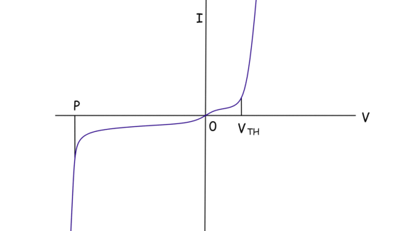 Positive V denotes forward bias under the plotted sign convention; negative V denotes reverse bias. When reverse-voltage magnitude is below VBR, a small leakage current flows. At VBR, avalanche or Zener breakdown causes reverse current to rise sharply and the external circuit must limit it. The breakdown value VBR is device-specific. A forward curve has no exact threshold: current changes exponentially over many decades. For a silicon diode, VF is often about 0.6 to 0.7 V at moderate current, but it varies with current, temperature, area and device construction.


