

- NMOS Logic Definition: NMOS logic is defined as a logic family using N-channel MOSFETs, offering higher density and speed for digital circuits.
- PMOS Logic Definition: PMOS logic is defined as a logic family using P-channel MOSFETs, which perform logic functions using positive and negative voltages.
- PMOS Inverter Function: In PMOS logic, an inverter uses a P-channel MOSFET as a load, with GND representing logic ‘1’ and -VDD representing logic ‘0’.
- NMOS Advantages: NMOS logic is preferred for its smaller chip area and higher speed due to better charge carrier mobility.
- Logic Gate Variations: NMOS logic includes variations like VMOS, DMOS, and HMOS, aimed at reducing propagation delay and improving performance.
The logic families we’ve discussed are used for discrete logic functions like logic gates, flip flops, counters, multiplexers, demultiplexers etc. These are found in simpler digital ICs at small-scale and medium-scale integration levels.
TTL, CMOS, and ECL logic families aren’t suitable for digital ICs with large-scale integration (LSI) complexity. For LSI-class digital ICs, PMOS, NMOS, and integrated injection logic (I2L) are used. We’ll discuss PMOS and NMOS here.
PMOS Logic
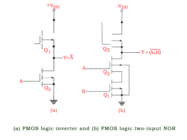
The PMOS logic family uses P-channel MOSFETS. Figure (a) shows an inverter circuit using PMOS logic (not to be confused with a power inverter). MOSFET Q1 acts as an active load for the MOSFET switch Q2. For the circuit shown,
GND and −VDD respectively represent a logic ‘1’ and a logic ‘0’ for a positive logic system. When the input is grounded (i.e. logic ‘1’), Q2 remains in cut-off and −VDD appears at the output through the conducting Q1. When the input is at −VDD or near −VDD, Q2 conducts and the output goes to near-zero potential (i.e. logic ‘1’). Figure (b) shows a PMOS logic based two-input NOR gate. In the logic arrangement of Fig.(b), the output goes to logic ‘1’ state (i.e. ground potential) only when both Q1 and Q2 are conducting.
This is possible only when both the inputs are in logic ‘0’ state. For all other possible input combinations, the output is in logic ‘0’ state, because, with either Q1 or Q2 nonconducting, the output is nearly −VDD through the conducting Q3. The circuit of Fig.(b) thus behaves like a two-input NOR gate in positive logic.
It may be mentioned here that the MOSFET being used as load [Q1 in Fig. (a) and Q3 in Fig. (b)] is designed so as to have an ON-resistance that is much greater than the total ON-resistance of the MOSFETs being used as switches [Q2 in Fig. (a) and Q1 and Q2 in Fig.(b)].
NMOS Logic
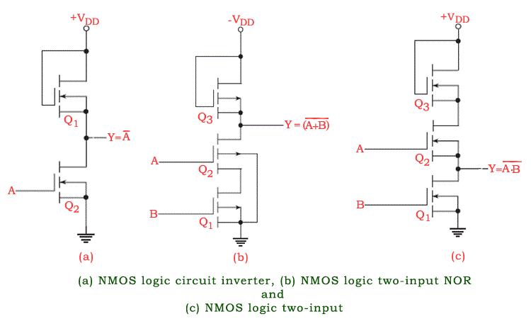
The NMOS logic family uses N-channel MOSFETS. N-channel MOS devices require a smaller chip area per transistor compared with P-channel devices, with the result that NMOS logic offers a higher density. Also, owing to the greater mobility of the charge carriers in N-channel devices, the NMOS logic family offers higher speed too.
This is why most MOS memory devices and microprocessors use NMOS logic or its variations like VMOS, DMOS, and HMOS. These variations aim to reduce propagation delay. Figures (a), (b), and (c) show an inverter, a two-input NOR, and a two-input NAND using NMOS logic.


")
