

- Extrinsic Semiconductor Definition: An extrinsic semiconductor is defined as a semiconductor with added impurities to increase its conductivity.
- Doping Process: Doping involves adding impurities to a pure semiconductor to create more free charge carriers.
- n-Type Semiconductors: n-Type semiconductors are created by adding Group V elements, which donate extra electrons.
- p-Type Semiconductors: p-Type semiconductors are formed by adding Group III elements, which create holes by accepting electrons.
- Conductivity in Extrinsic Semiconductors: The added impurities in extrinsic semiconductors increase their conductivity by creating more free electrons or holes.
Semiconductors are classified as intrinsic or extrinsic. Intrinsic Semiconductors are pure, while extrinsic semiconductors have added impurities. Doping, the process of adding impurities, increases the material’s conductivity by creating more free charge carriers, such as electrons or holes.
Pure semiconductors like Silicon (Si) or Germanium (Ge) are tetravalent, having four electrons in their valence shell. To increase the number of electrons, they are doped with Group V elements like Phosphorous (P) or Arsenic (As). Group V elements are pentavalent, meaning they have five valence electrons, leaving one free electron after forming four covalent bonds.
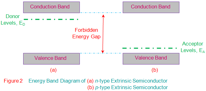
In other words, pentavalent impurities are said to donate their electron to the tetravalent (pure) semiconductors and are hence called donors. The electron so donated will be very loosely bound to its parent atom and can thus be made ‘free’ by supplying very minimal amount of thermal energy. Such an excitation causes the electron to transit from its current energy state, donor level ED (green line in Figure 2a) to the conduction band. From then on it can actively contribute to the process of conduction in the semiconductor material along with the other free electrons generated due to the breaking of covalent bonds. From this, one can note that the total number of electrons in such a material is the sum of thermally generated electrons and the electrons donated by the donor atoms.
However, the number of holes in the same material remains equal to the number of thermally generated electrons only. This indicates that the number of electrons in this kind of material exceeds the number of holes, which means the electrons will be the majority charge carriers while the holes will be the minority carriers. Thus, these materials are aptly named as n type semiconductors.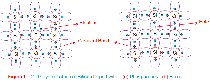
Group IV elements can be doped with Group III elements like Boron (B) or Aluminum (Al). These trivalent elements have three valence electrons, forming three covalent bonds but leaving one bond unfilled, creating a hole. This hole can accept an electron, making the material conductive.
The number of holes formed equals the number of trivalent impurity atoms added to the semiconductor. These holes, present at energy level EA, can readily accept electrons. Because these holes accept electrons, Group III elements are called acceptors.
Moreover, it is to be noted that, as an electron moves into the hole to recombine, it leaves a new hole in its previous place which in turn will be filled by some other electron. This indicates that the movement of electrons in one direction can be viewed as the movement of holes in the opposite direction. Thus, such a semiconductor material becomes conductive in nature. However, it is to be noted that, for this case, the total number of holes will be equal to the sum of the holes induced due to doping and the holes generated due to the thermal excitation process, unlike the electrons which are produced only due to the process of thermal excitation. This means that here the number of holes exceeds the number of electrons for which the holes will be the majority charge carriers while the electrons will be the minority charge carriers. Due to these kinds of extrinsic semiconductor materials are aptly called p type semiconductors.


