

- Fan Out Definition: Fan out in digital electronics is the maximum number of inputs a single logic gate output can drive without causing errors.
- Current Sourcing and Sinking: Logic gates must source or sink current based on their high or low output state to drive other gates.
- Fan Out Calculation: Fan out is IOH/IIH when the output is high and IOL/IIL when the output is low, ensuring the logic gate can drive multiple inputs.
- Circuit Design Importance: Proper fan out ensures that circuits function correctly without overloading any logic gate, which is essential in circuit design.
- TTL Logic Family: TTL logic gates have specific fan out values that must be considered when designing circuits.
Fan-out in digital electronics is the number of same-family gate inputs that one logic-gate output can drive without leaving the valid logic levels. One output can feed several inputs, but only up to that count.
The limit is set by how much current the output can source at a high level and how much current it can sink at a low level, compared with what each driven input draws.
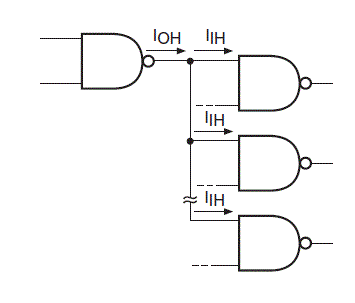
The diagram below is a worked high-level case.
The current sourcing capability of a NAND gate is IOH when its output is high, and each driven input takes IIH. The largest number of inputs that output can feed is IOH/ IIH. That ratio applies in the high state. When the output is low, take the largest sink current as IOL. Each connected input then draws IIL. The next diagram shows that case.
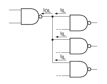
In this case the largest number of inputs is IOL / IIL. One gate output can therefore feed IOH / IIH inputs when high and IOL / IIL inputs when low.
That count is the fan-out. Using it keeps a driven node inside the legal high and low bands. Fan-out is a listed rating in digital electronics.
When IOH/IIHand IOL / IIL are not equal, the smaller ratio is taken as Fan Out of Logic Gates and the load count uses that value.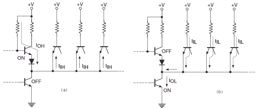
The two figures show a circuit where the output of a single NAND gate in a standard TTL (Transistor Transistor Logic) family feeds several NAND inputs of the same family.
The first figure is the high output state and the second is the low output state. For standard TTL family devices the maximum high-state output source current and the maximum high-state input current are 400 mu A and 40 mu A respectively. The low-state figures are 16 mA and 1.6 mA. Other pages on this site cover TTL in more detail.


